-
 Anglický jazyk
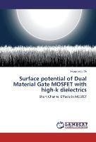
Surface potential of Dual Material Gate MOSFET with high-k dielectrics
Autor: Swapnadip De
The shrinking of device dimension leads to reduction of gate oxide thickness. As a result of this the undesirable hot electron effect and the gate tunneling current is increased. In order to overcome this drawback high-k materials are used instead of silicon... Viac o knihe
Na objednávku, dodanie 2-4 týždne
33.30 €
bežná cena: 37.00 €
O knihe
The shrinking of device dimension leads to reduction of gate oxide thickness. As a result of this the undesirable hot electron effect and the gate tunneling current is increased. In order to overcome this drawback high-k materials are used instead of silicon dioxide as the insulating material underneath the gate. High-k dielectrics are used in semiconductor manufacturing processes where they are usually used to replace a silicon dioxide gate dielectric.Among various high-k materials, Hafnium oxide (HfO2), Tantalum pent oxide (Ta2O5) these materials appear to be the candidates for replacing silicon oxide. These high-k dielectrics exhibit a trend of decreasing barrier height with increasing dielectric constant.The high-k materials with far higher permittivity create same gate capacitance for thicker dielectric. In this book the main focus has been on the modeling and the influence of depletion layers around the source and the drain regions on the sub threshold surface potential of a short-channel DMG MOS transistor with a uniformly-doped channel.
- Vydavateľstvo: LAP LAMBERT Academic Publishing
- Rok vydania: 2013
- Formát: Paperback
- Rozmer: 220 x 150 mm
- Jazyk: Anglický jazyk
- ISBN: 9783659421228


 Nemecký jazyk